
Key takeaways
- An FPGA is a reconfigurable chip that executes trading logic directly in hardware with deterministic, nanosecond-level latency.
- FPGAs typically handle network processing, market data parsing, order book building, pre-trade risk checks and order generation.
- Published benchmarks show FPGA tick-to-trade paths in the tens of nanoseconds, versus low single-digit microseconds for optimised software.
- Development uses hardware languages (Verilog/VHDL) or high-level synthesis from C++; build times of hours and scarce talent are the main constraints.
- FPGAs pay off where latency directly decides P&L — market making and arbitrage on contested venues; elsewhere, kernel-bypass software is usually enough.
What is an FPGA and why do trading firms use it?
An FPGA (field-programmable gate array) is a chip whose circuits can be reconfigured to run specific logic directly in hardware. Trading firms use FPGAs to process market data and send orders in nanoseconds with almost no timing variation — something general-purpose CPUs, with their operating systems and caches, cannot match.
A CPU executes instructions one after another, sharing resources between many tasks. An FPGA is a grid of logic blocks, memory and high-speed transceivers that engineers wire together for a single purpose. Every packet follows the same hardware path, every time.
That determinism is as valuable as raw speed. In a latency race, a system that is fast on average but occasionally slow will lose unpredictably. FPGAs remove most of that variability.
Why FPGAs replaced CPUs on the critical path
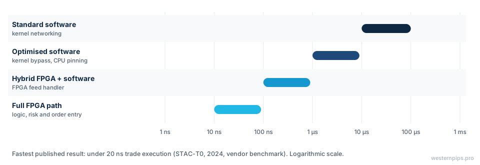
As networks approached the speed of light and kernel-bypass software reached low single-digit microseconds, the remaining delay sat inside the server. FPGAs eliminated the operating system, PCIe transfers and software overhead from the critical path, cutting tick-to-trade from microseconds to tens of nanoseconds.
The evolution of the trading critical path:
| Generation | Typical tick-to-trade | Key technology |
|---|---|---|
| Standard software | Tens of microseconds | Kernel networking |
| Optimised software | Low single-digit microseconds | Kernel bypass, CPU pinning |
| Hybrid FPGA + software | Sub-microsecond | FPGA feed handler, software strategy |
| Full FPGA path | Tens of nanoseconds | Logic, risk and order entry in hardware |
AMD and Exegy reported a STAC-T0 result in 2024 with trade execution times below 20 nanoseconds on an FPGA platform. Vendor benchmarks should be read carefully, but they show where the frontier is.
Figure 1: Tick-to-trade latency by architecture
What runs on the FPGA
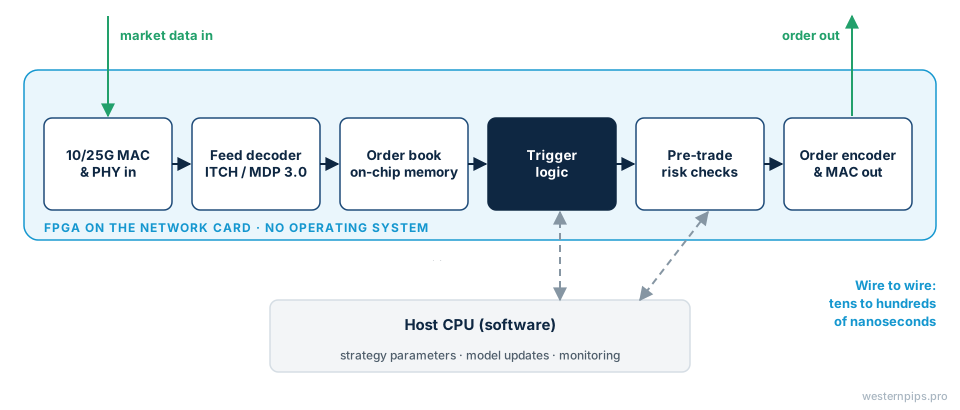
A trading FPGA usually handles the network stack, market data decoding, order book maintenance, simple trigger logic, pre-trade risk checks and order encoding. More complex decision-making, parameter updates and monitoring stay in software on the host CPU.
Figure 2: The tick-to-trade pipeline inside an FPGA
Feed handlers and book building
The FPGA receives multicast market data directly from the network, decodes the exchange’s binary protocol — such as ITCH or CME MDP 3.0 — and updates an order book in on-chip memory. Because it processes packets as they stream in, it can act before the full packet has even arrived.
Trigger logic, risk checks and order entry
Simple strategies — “if the best bid on venue A moves by one tick, update or cancel my quote on venue B” — can be evaluated in hardware. Regulatory pre-trade risk checks, such as price collars, size limits and credit checks required under rules like SEC Rule 15c3-5, can also run in the FPGA so they add only nanoseconds. Finally, the FPGA builds the order message and transmits it.
Development workflow: RTL versus HLS
FPGA logic is written either in register-transfer-level languages such as Verilog and VHDL, which give precise control over timing, or through high-level synthesis, which compiles C++ into hardware. Most teams combine both: HLS for productivity, RTL for the most latency-critical blocks.
The workflow differs sharply from software development:
- Design in RTL or HLS.
- Simulate and verify extensively — bugs in hardware are expensive and hard to observe.
- Synthesise, place and route — builds can take several hours for a large design.
- Timing closure — ensuring every signal meets the clock deadline.
- Deploy and test on the target card with recorded market data.
Long build cycles and the scarcity of engineers who understand both hardware and trading are the main reasons FPGA projects are expensive.
FPGA hardware platforms
The FPGA trading market is dominated by AMD (formerly Xilinx) and Intel’s Altera devices, delivered on accelerator cards and smart NICs. AMD’s Alveo UL3524 and UL3422 cards target ultra-low latency trading, and layer-1 switches with embedded FPGAs extend the approach into the network itself.
| Platform type | Role | Notes |
|---|---|---|
| FPGA accelerator card (PCIe) | Full trading path or feed handling | Most common form factor |
| Smart NIC with FPGA | Network offload plus custom logic | Bridges software and hardware |
| FPGA-enabled layer-1 switch | Data fan-out, filtering, simple logic | Logic in the network itself |
| Vendor trading platforms | Pre-built feed handlers, risk, order entry | Faster time to market |
FPGA versus ASIC
An ASIC is a custom chip built for one design. It can beat an FPGA on speed and power, but development costs millions and takes a year or more, and the logic cannot change. In trading, where exchange protocols and strategies evolve constantly, the FPGA’s reprogrammability usually wins.
ASICs make sense only for extremely stable, very high-value functions. Most firms reserve them, if at all, for components such as network processing where requirements rarely change.
Team, cost and time to market
The hardware is the smallest cost of FPGA trading. Specialised engineers, verification, toolchain licences and long build-test cycles dominate. Many firms therefore buy vendor platforms or IP cores for feed handlers and order entry and focus in-house effort on the logic that differentiates them.
Cost drivers to plan for:
- Talent: FPGA engineers with trading experience are scarce and expensive.
- Tooling: synthesis tools, simulators and test infrastructure.
- Exchange changes: every protocol update means new hardware builds and certification.
- Opportunity cost: slower iteration than software strategies.
Vendors argue that buying platforms saves time and money compared with in-house builds; firms with unique strategies often still build their own critical-path logic.
When FPGAs are — and are not — worth it
FPGAs pay off when latency directly determines profit: market making and arbitrage on contested venues, where losing races by nanoseconds costs real money. For execution algorithms, slower strategies or most FX and crypto workflows, optimised kernel-bypass software usually delivers enough speed at a fraction of the cost.
A quick decision checklist:
- Do you compete in races decided by less than a microsecond? Consider FPGAs.
- Is your logic simple and stable enough to express in hardware? FPGAs fit.
- Does your strategy change weekly or depend on complex models? Stay in software.
- Is network latency to the venue still in milliseconds? Fix the network and colocation first.
Frequently asked questions
How are FPGAs used in trading?
FPGAs run the most latency-sensitive parts of a trading system in hardware: receiving network packets, decoding exchange market data, maintaining the order book, evaluating simple trading logic, running pre-trade risk checks and sending orders — all within nanoseconds and with very consistent timing.
Are FPGAs faster than CPUs for trading?
For simple, fixed logic on the critical path, yes — typically by one to two orders of magnitude, and with far lower jitter. CPUs remain better for complex strategies, research models and anything that changes frequently.
What is the difference between an FPGA and an ASIC?
An FPGA can be reprogrammed after manufacture; an ASIC is a custom chip built for one design. ASICs can be faster and more power-efficient but cost far more and take much longer to develop, so they make sense only for very stable, very high-value logic.
Can FPGA trading logic be written in C++?
Yes, through high-level synthesis (HLS) tools that compile C or C++ into hardware designs. HLS speeds up development, but the most latency-critical paths are still often written in Verilog or VHDL for maximum control.
How much does FPGA trading infrastructure cost?
Accelerator cards cost thousands to tens of thousands of dollars each, but the main cost is engineering: specialised hardware developers, verification, toolchain licences and long build-test cycles. Many firms buy vendor platforms rather than building everything in-house.
Sources and further reading
- How are FPGAs used in trading? — IMC Trading
- Ultra-low latency trading: how low can you go? (sponsored, AMD; STAC-T0 results) — Risk.net, 2024
- STAC-T0 benchmark — STAC (Securities Technology Analysis Center)

Svetlana Berezhnova is a co-founder of Westernpips and has been a trader since 2007. She has been with the company from its very beginning and is an expert in high-frequency trading and latency-sensitive trading software.
This article is for educational purposes and describes market structure; it is not investment, legal or tax advice. Statistics are attributed to their original sources, which should be consulted for methodology and limitations.